

PRODUCTS
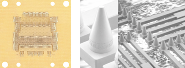
Pad Socket
Built with 3D MEMS fabrication, this horizontal cantilever structure uses a probe to make precise contact with the pad for testing.
Applications
- Memory (HBM etc.,)
- System Logic (GPU, CPU, ASIC, SoC)
- System Level Test
| Category | Detail | Spec. |
|---|---|---|
| Mechanical | Pitch (μm) | 100 - 150 |
| Stroke(OD) (μm) | 50 - 100 | |
| Thickness (mm) | 4.5 | |
| Contact Force (gf/pin) | 5 ± 2.0 | |
| PPA(Pin Position Accuracy) (μm) | ±3.0 | |
| Electrical | Contact Resistance (mΩ) | <150 |
| Current (A) | 1.2 |
Product Portfolio
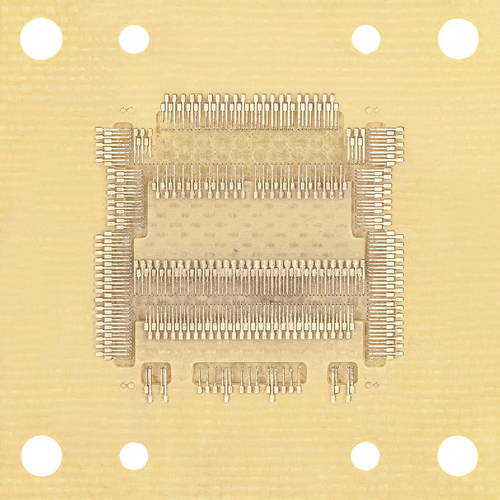 Contactor/Die socket
EDS Pad Contact
Available as a standalone contactor or integrated with a PCB as a die socket.
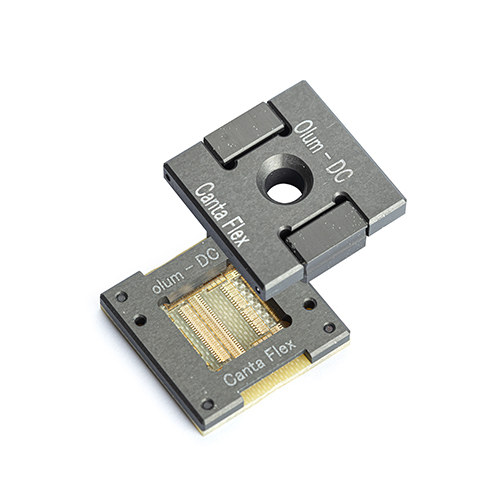 Die carrier
Die Carrier for ATE Applications
Enables precise die positioning and alignment during automated semiconductor testing